Researchers Use an EUV Flashlight and Free-Air Diffusion, Plus a Clever Algorithm, to Inspect Chips
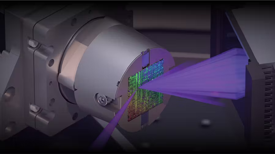
Postdoc Yifeng Shao (ImPhys) and his colleagues from Delft and Utrecht University have investigated a new imaging technique using extreme ultraviolet light to study the three-dimensional structures of chips at the nanoscale.
When you're playing with extreme ultraviolet light, lenses aren't going to cut it — but a TensorFlow-accelerated algorithm will.
The work has been published in Nature Light: Science & Applications. Hackster.io wrote an article about the study: “When you're playing with extreme ultraviolet light, lenses aren't going to cut it — but a TensorFlow-accelerated algorithm will.”
Abstract
Ptychographic extreme ultraviolet (EUV) diffractive imaging has emerged as a promising candidate for the next generationmetrology solutions in the semiconductor industry, as it can image wafer samples in reflection geometry at the nanoscale. This technique has surged attention recently, owing to the significant progress in high-harmonic generation (HHG) EUV sources and advancements in both hardware and software for computation. In this study, a novel algorithm is introduced and tested, which enables wavelength-multiplexed reconstruction that enhances the measurement throughput and introduces data diversity, allowing the accurate characterisation of sample structures. To tackle the inherent instabilities of the HHG source, a modal approach was adopted, which represents the cross-density function of the illumination by a series of mutually incoherent and independent spatial modes. The proposed algorithm was implemented on a mainstream machine learning platform, which leverages automatic differentiation to manage the drastic growth in model complexity and expedites the computation using GPU acceleration. By optimising over 200 million parameters, we demonstrate the algorithm's capacity to accommodate experimental uncertainties and achieve a resolution approaching the diffraction limit in reflection geometry. The reconstruction of wafer samples with 20-nm high patterned gold structures on a silicon substrate highlights our ability to handle complex physical interrelations involving a multitude of parameters. These results establish ptychography as an efficient and accurate metrology tool.