Could we use the light emitted by atomic defects in 2D materials as sensitive nano sensors to sequence biomolecules such as DNA and proteins? With this technology, we could improve the diagnosis, prevention, and treatment of diseases such as cancer. For his master's thesis, High-Tech Engineering student Tetsuo Martynowicz focuses on the role of strain in the properties of these atomic defects.
What exactly are you researching?
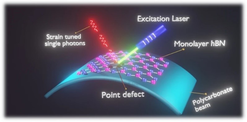
I am researching how strain affects the properties of tiny light sources called quantum emitters in atomically thin 2D materials like hexagonal boron nitride (h-BN). With this, I am trying to control the location and colour of these light sources at the nanometre scale (similar to the size of an atom). We can create defects in the crystal structure of h-BN by removing atoms or introducing new elements. When you shine a laser on these defects they will return light packages called photons. This phenomenon, called quantum emission, happens because of the unique electronic structure in these defects. To make these light emitting defects useful in real world applications, we must control their location and emitted colour. I am applying strain to the material, thereby deforming the electronic structure of the defects, to investigate its effect on their emission properties.
Why is this important?
The light emitted by these defects can be used for various applications such as quantum computing, communication, and sensing. The research group I work in focuses on using these defects as a nano sensor to sequence and identify biomolecules such as DNA and proteins. These biomolecules play an essential role in the health and functioning of cells and accurately monitoring them can help improve diagnosing, preventing, and treating diseases such as cancer.
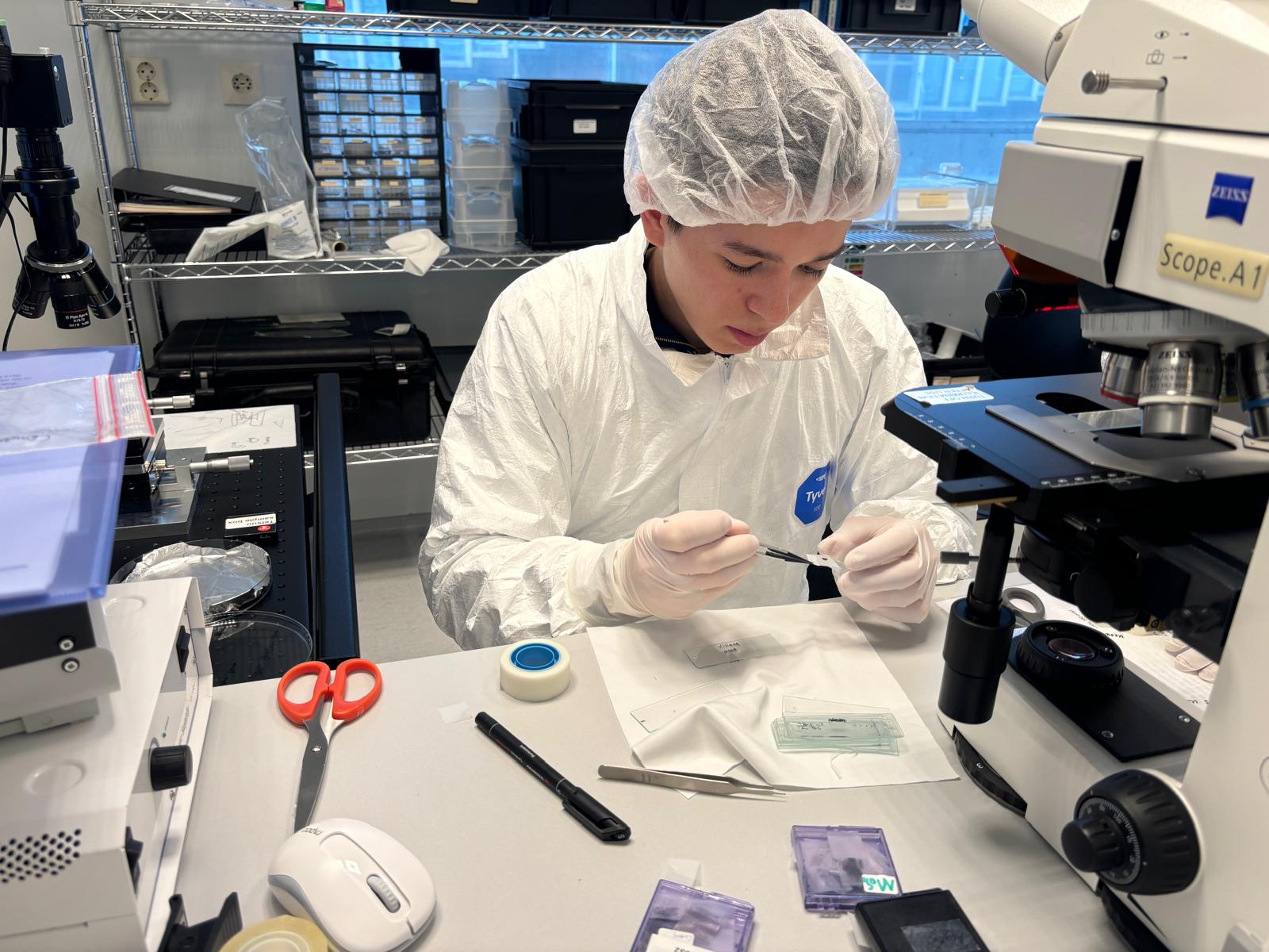
Can you describe your research method?
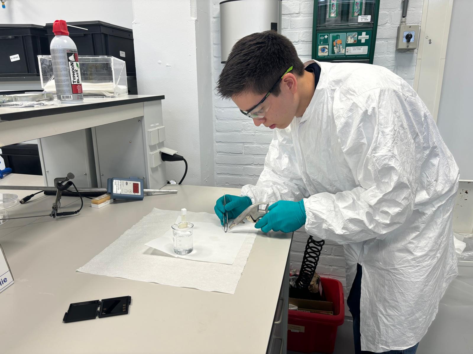
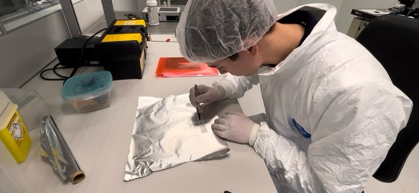
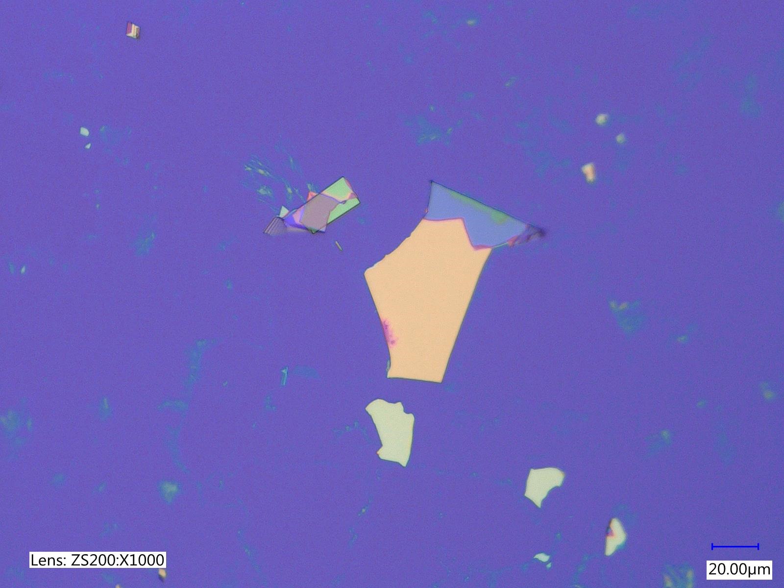
Firstly, I will peel the bulk h-BN crystal into a few-layer flake using adhesive tape. Then, the flake is transferred to a silicon chip, which is similar to a chip in your phone or computer. Secondly, I will create defects in the h-BN by bombarding the flake with ionised oxygen gas. These ions have enough energy to knock-out atoms from the crystal surface. Thirdly, I heat up the plasma treated chip to around 850 C. Because h-BN and silicon have different thermal expansion coefficients, strain is induced in the h-BN when heating up and cooling down. Lastly, I will use different measurement devices and microscopes to quantify the strain in the material and to analyse the location and colour spectrum of the emitted light by the defects.
What were you most looking forward to beforehand?
I have always enjoyed practical work during my bachelor and master, so what made me particularly excited for this project was the combination of theory and practical work to independently fabricate and analyse samples in the labs. It gives me a great sense of ownership over my project and it serves as a nice opportunity for learning and gaining hands-on experience with highly advanced equipment.
What will be your biggest challenge?
I have little experience in nanoscience. It really pushes my understanding of physics and it requires me to think completely different from a classical macro-scale mechanical engineering point-of-view. In addition, I need to get familiar with a wide range of fabrication and measurement techniques that are fairly new to me.
What is the most important thing you have learned so far?
It is a cliché, but if you work on a project you’re passionate about and that really sparks your curiosity you will have a much easier time. It also helps to keep your literature organised.
What have you enjoyed the most so far?
I have enjoyed the process of studying literature and diving into the nanoworld a lot. The physics at this scale is fascinating and sometimes hard to grasp. Also working and learning new skills in the labs has been very interesting and great fun.
What is the next step?
In order to make quantum emitters in 2D materials a practical technology for protein sequencing, much more research is required. For example on the energy transfer between proteins and emitters, and the transport of molecules across the h-BN surface.
Tell us about your plans for the future
It has been a dream of mine to join the Dutch military, so I hope to pursue that goal after my graduation. After a few years, I intend to continue my career at a company in the high-tech industry.
Study related
Why did you opt for Mechanical Engineering in general and High-Tech Engineering in particular?
At first I was not sure what I wanted to study, but eventually I settled on mechanical engineering because it provides you with a solid foundation in math, mechanics, dynamics, and analytical thinking and there are many fun project-based courses in which you learn to design and build systems. Luckily, this turned out to be a good decision. For my master I chose High-Tech Engineering since it is a comprehensive study program with many different fields to specialize in. The common goal of research in these fields is to maximize the performance of systems in terms of speed, precision, mass, and energy consumption which I find really cool and interesting from an engineering point of view.
In what way did your Mechanical Engineering bachelor help you?
It helped me develop problem-solving skills, critical thinking, and the tools to set up a research project.
Which parts of your Mechanical Engineering master can you apply?
In contrast to the bachelor's program, as a master's student you are more reliant on yourself and are expected to take on more responsibility. This starts with putting together your course program, receiving less guidance from TAs, and arranging your own thesis. I think this unconsciously developed independence has helped me with setting up my thesis and gaining the confidence that I can successfully complete it.